Implementing the DN6678 CPU using an FPGA
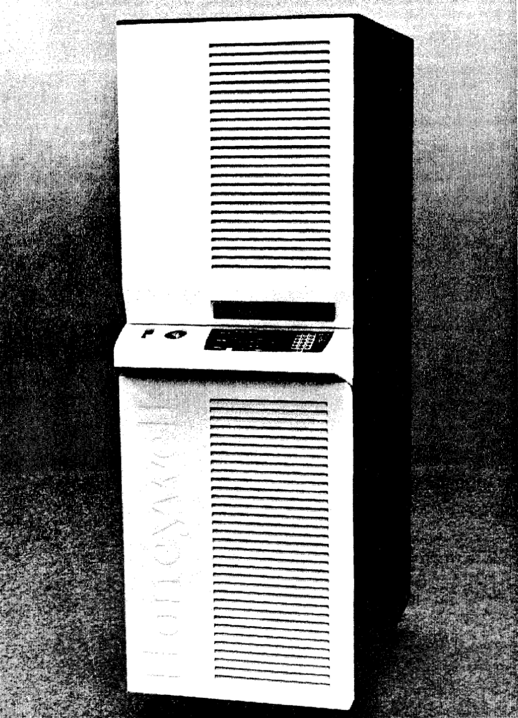
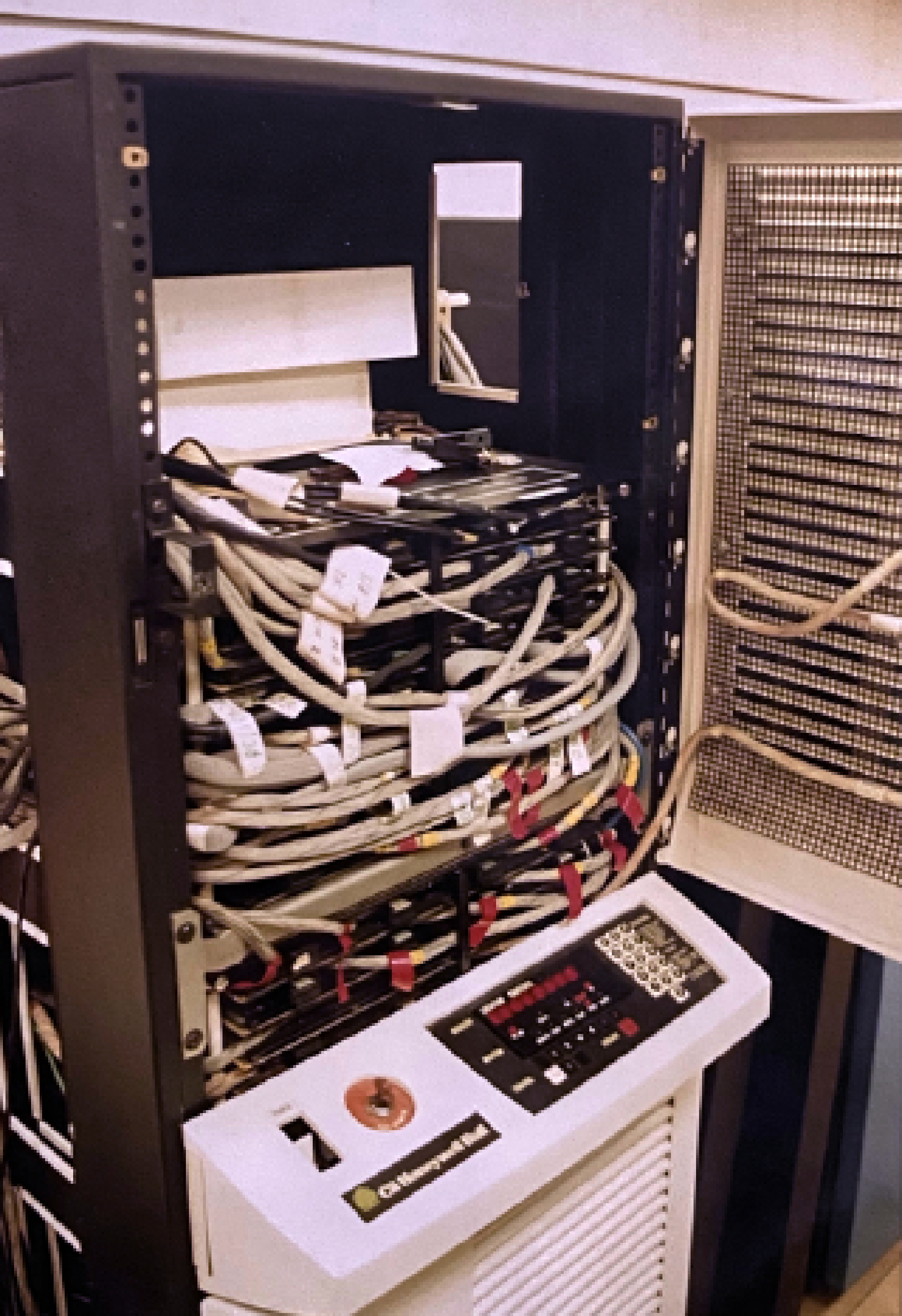
This post is going to discuss some of the specifics of the FPGA implementation of the Honeywell DATANET 6678 Front-End Network Processor.
First off, one of the main goals of this project, aside from achieving the end result, is to gain a thorough understanding of FPGA design and programming. To help accomplish this goal, I am reading the book “Computer Architecture Tutorial Using an FPGA” by Robert Dunne. This book provides excellent tutorials on FPGA programming using Verilog with the Terasic DE-10 Lite development board and offers a detailed guide on implementing a 32-bit ARM processor. I highly recommend this book.
Let’s take a quick look at the top-level schematic of the FNP. (You can click on the image for a zoomable version.)
-
Reset Timer: This module provides a
RESETsignal that lasts 1,024 clocks to make sure everything has settled down. Note that the FPGA board is providing a 50 MHz clock. -
IOM Module: The IOM (Input/Output Multiplexor) does all the heavy lifting of I/O processing for the FNP. It also contains the Interrupt Control Module (though this may change in the future).
-
UART: The UART provides a serial input/output that can be interfaced to either an RS‑232 port (via level converters and drivers) or to a USB serial interface (which is how we are currently using it). This port will initially be used to provide a console for the FNP, however, the plan is to make it a multiplexed interface to allow several serial devices to access the FNP.
-
CPU Module: This, of course, is the main CPU (Central Processing Unit) for the FNP. It implements the Honeywell DN355 instruction set and we will dive deeper into it later.
-
Memory Pager: This module sits between the CPU and the Block RAM and provides access to more than 32KW (kilowords) of memory. With the available Block RAM, this implementation has 64KW available.
-
Mailbox Detector: This module determines when a Mailbox (communication register) is accessed (as opposed to a RAM location). This is important as there are many special Mailbox locations used to communicate with the various hardware elements (basically, implementing memory-mapped I/O).
-
Dual Port Block RAM: The DE10‑Lite provides dual ported Block RAM that can be split up for multiple purposes. Currently, only one port is used. We have some thoughts about using the second port for debugging. (At one time, we considered using the second port for the IOM, but since the memory pager needs to be accessible for the IOM as well, this idea has been discarded.)
-
Display Module: This module just interfaces with the 6 seven-segment LED displays on the DE10‑Lite board. Using switches, you can examine the various registers in the CPU (as well as some IOM signals).
Note there is some additional “glue” logic in the diagram that I have not described. It is not too important, or at least, not relevant to the CPU discussion.
Now let’s look at the CPU module itself. (You can click on the image for a zoomable version.)
-
ALU Module: Of course, any reasonable CPU design needs an ALU (Arithmetic Logic Unit). This module is responsible for almost all of the math and logical operations the CPU needs to perform. This ALU has nine different operations (not counting the no‑op/null‑operation) and will be more fully described in a later post.
-
Adder 18: This is an 18‑bit adder that is used by the Memory Control for certain RMW (read-modify-write) memory operations, such as adding 1 to a given memory location. This adder allows for atomic RMW operations and accelerates these operations (rather than having the Operation Unit and ALU involved with every simple addition).
-
Memory Controller: This memory controller provides a lot of functionality. It can read or write 18 or 36 bits to and from memory, perform atomic RMW operations, and interface to the Memory Paging Unit. (Note that this module is going to be moved off of the CPU and into the new Memory Management Unit.)
-
ROM Init Binary: This is a chunk of Block RAM that gets “preloaded” with T&D (Test & Diagnostic) code when the FPGA is initially configured. Originally, this code was generated using a “mini-assembler” (see below), but is now built using 355MAP (the “DATANET 355/6600 Macro Assembler Program”, see DD01) running under Multics. Depending on a switch setting, this code can be copied to the start of RAM when the CPU is reset.
-
Instruction Decoder: This module will break down an instruction into various parts. It also determines which “Group” (see DD01) the instruction is in. (Note that originally this function was part of the Operation Unit. However, it was cleaner to implement the Operation Unit with the Instruction Decoder as separate module.)
-
Operation Unit: This is the heart of the CPU and is responsible for actually executing the instructions. It is a large state machine with twelve possible states for executing instructions. It also coordinates the activities of the Memory Controller and the ALU.
The rest of the logic on this board is responsible for presenting the CPU portion of the 6 seven-segment LED displays on the DE10‑Lite board. These signals go back to the Display Module on the top level board.
A problem that occurs when developing a CPU is to figure out how to execute “test code” that exercises newly implemented functionality. Dunne offers nice solution for this issue, in the form of a “mini-assembler”, implemented directly in Verilog, that allows you to write test code as if it was in an on-board ROM. Using this technique allowed for the coding of tests for each instruction as they were added to the CPU.
Eventually, enough of the architecture was implemented that it was possible to write the tests using the 355MAP assembler on Multics to build a load module that could be put into a simulated ROM, at which point the “mini-assembler” was removed.
Looking at the T&D code, you can observe how the instructions were implemented, and as each instruction was added, one or more tests were added to exercise the instruction.
If you examine the first part of the T&D code, you can see that the LDI instruction must work in order to mask interrupts, and we see the first test case:
Based on that comment, the ILA, TZE, TNZ, and TRA instructions were the first to be implemented.
In fact, the LDI instruction was first created as a no-op because interrupts were not yet implemented!. The very first working instruction was TRA (which “transfers execution” to another address, i.e. jumps). Without at least this instruction, it would be very hard to write any tests!
Once the unconditional TRA was working, the variants for transfer on ‘zero flag’ (TZE) and transfer on ‘not zero flag’ (TNZ) were implemented. Of course, to fully test the instruction, you need to be able to set these flags, which is what the ‘immediate load A’ (ILA) instruction does. And finally, we have our first fully working test!
The next instructions implemented were:
These instructions add comparison capabilities and the rest of the ‘transfer on flags’ functionality.
If you read through the rest of the T&D code, you can see the exact order the instructions and capabilities were implemented.
- DPS8M-HW - GitLab repository for the DPS‑8/M hardware FPGA project.
- Announcement - Hardware (FPGA) DPS-8/M ∕ FNP Project
- Discussions are hosted on the “Multiplexed Information and Computing Service” Slack workspace.
- Join the #hardware-emulation channel or request access to the Slack workspace.
— Dean S. Anderson


