
New Project:Hardware (FPGA) DPS-8/M ∕ FNP Project
We’re excited to announce an ambitious long-term project, currently in the early stages, to implement as much of the DPS‑8/M mainframe architecture as possible using one (or more) FPGAs — with the ability to run the full Multics operating system — is now underway, led by Dean S. Anderson.
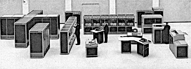
In the early 1980s, Dean started as a computer operator at Gelco on a large Honeywell Series‑60 ∕ Level‑66 dual processor mainframe (eventually converted to a four processor DPS‑8) running GCOS‑3. Over time, he worked his way through Gelco’s Production Control and Special Projects groups writing programs to automate the Computer Operations Department. This included writing GCOS‑3 kernel modifications for special handling of tapes.
In 1985, Dean went to Honeywell Underseas Systems Division where he coordinated PBX installations as well as wiring for both broadband and Ethernet networks. He also wrote a lot of software in C for automating factory floor operations and board assembly, and worked on other large projects, including networking a significant number of Level 6 minicomputers.
Currently, Dean is a Principal Software Architect for Tabula Rasa Healthcare.
As a member of the DPS8M Development Team, Dean authored the ‘punutil’ utility for punched card manipulation and conversion. Additionally, Dean made important contributions to the DPS8M Simulator, specifically in the areas of magnetic tape and unit record equipment (e․g․ card reader, card punch, printer) handling, as well as automated testing.
The following is Dean’s update on the ongoing work.
In November of 2021, I was looking for a long-term hobby project, and I was seeing a lot of different work happening on FPGA implementations of historic minicomputers and mainframes such as the IBM System/360.
I had already been working with the awesome DPS8M Simulator and Multics for some time, since I have a history as an operator/programmer/system programmer on Honeywell “Large Systems” mainframes running GCOS‑3 (Level‑66 & DPS‑8).
While there are quite a few people working on IBM S/360 and CDC simulation and emulation, there is unfortunately little being done for our favorite 36‑bit GE Large Systems / Honeywell / Bull 600/6000‑series systems. Since I’ve always been interested in FPGA development (and previously played around with it a bit), I decided my long-term hobby project would be to implement the complete DPS‑8/M distributed processing mainframe architecture in one or more FPGAs.
I expect this to be a very long project as I currently work a regular job and I’m at least several years from retirement. I also have a few health issues that can slow me down at times. For anyone expecting a fully working FPGA emulation of the DPS‑8/M in the very near future, don’t hold your breath just yet!
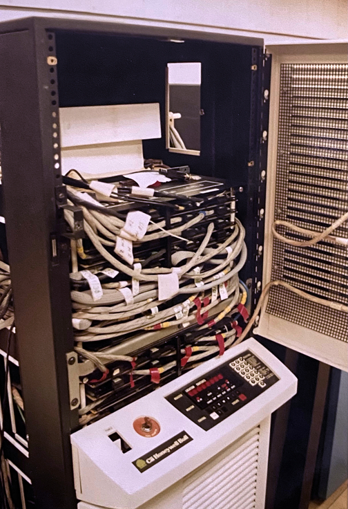
After some discussion, I decided that first implementing the FNP (Front-end Network Processor) component, specifically, the DATANET 355 (or DN355), also known as the DN6632 (denoting it’s 32 KW of memory), would be the ideal starting point. These systems have a simpler 18‑bit processor than the primary 36‑bit DPS‑8/M CPU, and would provide a suitable way to learn Verilog.
As the FNP CPU can be thought of as a simplified “half a DPS‑8 CPU”, while also having similarities to the central system (including an IOM, Input/Output Multiplexer) in a simplified form, the experience gained working on this component should be transferable to the system as a whole.
Enter Charles Anthony — a truly awesome programmer who did amazing work on the DPS8M Simulator — who already had a partial FNP emulation, coded in C99. This code originated from the DPS8M Simulator, but was abandoned in favor of a simpler (yet more robust and better performing) FNP simulation; that is, a native-code reimplementation, handling the commands sent to/from the FNP from the DPS‑8 directly, instead of emulating the instruction set of the 18‑bit FNP CPU and running the genuine MCS (Multics Communication System) software on it.
Charles suggested that he complete the FNP emulation software to aid in the development of the FPGA system. However, we soon discovered that the MCS of the late 1980’s had grown, and no longer supported the original DN355 FNP, but only the later DN6661/DN6670/DN6678 models, that is, those equipped with more than 32 KWords of memory.
We changed our designs to target this system. This was not a major change, but it meant the software emulation (and the FPGA, eventually) needed to implement the memory paging unit that allows the processor to access memory over the 32 KW boundary.
The FNP emulation software, DATANET6600, is now available and mostly complete (lacking a complete IOM implementation), and has been essential in the development of the FNP FPGA.
Charles proposed selecting an FPGA that incorporated an onboard ARM CPU core. This approach would allow us to begin with the DPS8M Simulator software running on the ARM core, and gradually replace sections of the software code with Verilog FPGA implementations until all elements have been transitioned from the ARM to the FPGA.
This resulted in the need for a requirements definition for the target development board to use. I had already explored and experimented with boards from Digilent (Nexys series) and Terasic (DE series).
Ultimately, I decided on the Terasic DE series.
|
|
|
The Terasic DE series was selected for the following reasons:
-
It uses FPGAs that support development using Intel Quartus Prime, a very nice IDE for FPGA development, which includes a free version that is adequate for our needs.
-
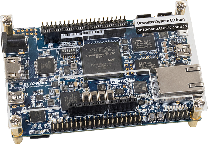
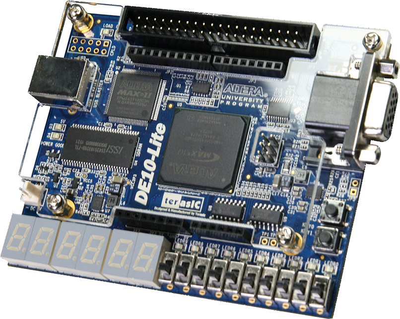
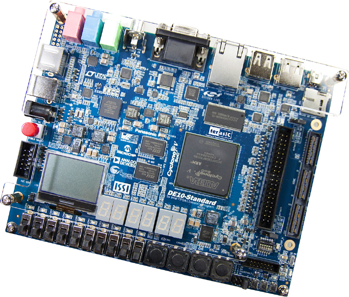
There are three very good development boards in the DE‑10 series: the DE10‑Standard, DE10‑Lite, and DE10‑Nano. I especially liked the DE10‑Nano since it has a history with the MiSTER project, emulating a large number of microprocessors, classic computers, and arcade games.
-
The DE10‑Standard and DE10‑Nano boards in the series are offered with ARM-based hardware processors.
-
I already owned a DE10‑Lite board for evaluation and used it to complete a tutorial on Verilog.
While the DE10‑Standard can be used to support development, because there is no explicit need for the ARM core in the finished DN6678 FNP, and because I feel that the DE10‑Nano simply won’t be enough to support a fully featured mainframe alone, I decided to target the DE10‑Lite for the FNP (as well as the mass storage, tape, and unit record processor) components. With the FNP handled, (hopefully) two complete DPS‑8/M CPUs will be able to be implemented using one DE10–Nano (along with a 12 MWord SCU and an IOM).
This way an entire Honeywell / Bull Distributed Processing System mainframe can be assembled from these components.
Where do things stand currently?
- DN6678 CPU
- Paged RAM
- The paged RAM is implemented in Block RAM on the FPGA and provides 64 KWords (18 bit words) of storage.
- There is a working implementation of the paging unit, but, when working with the IOM implementation, there are a few issues which will require some restructuring to handle things like mailbox reads/writes from/to the IOM boards.
- IOM
- The IOM in this design contains the simulation for various plug-in boards.
- While some of the concepts of the plug-in boards will be simulated, the actual population of these boards will be fairly fixed and require re-working of the Verilog code to change what boards are present.
- This is due to the fact that we will not need to provide hundreds of serial ports to run a large number of terminals.
- The IOM Central is partially implemented as well as the elapsed and interval timers.
- Interrupt Controller
- The IOM in this design also contains the Interrupt Controller which is fully implemented.
-
DPS8M-HW - GitLab repository for the DPS‑8/M hardware FPGA project.
-
DATANET6600 - DATANET 6600-series Front-end Network Processor emulation software.
-
Discussions are hosted on the “Multiplexed Information and Computing Service” Slack workspace.
- Join the #hardware-emulation channel or request access to the Slack workspace.
— Dean S. Anderson